

size restrictions exist for PCB prototypes
When designing a PCB prototype, one of the important factors to consider is the size of the printed circuit board itself. The size restrictions for PCB prototypes can vary based on several factors, including the manufacturer, the type of PCB, and the complexity of the design. Understanding these size limitations is crucial in ensuring that your prototype can be fabricated and assembled efficiently, while also meeting the functional and design requirements of your project. While there is flexibility in terms of size, there are certain constraints and considerations to keep in mind.
The first consideration when determining the size of a PCB prototype is the capabilities of the PCB manufacturer. Different PCB manufacturers offer different maximum and minimum board sizes for prototyping. Typically, the standard size for a PCB prototype is around 100mm x 100mm (4 inches x 4 inches), but many manufacturers can accommodate larger or smaller sizes depending on their equipment and processes. Some manufacturers may offer larger PCBs up to 400mm x 400mm (15.7 inches x 15.7 inches) or even larger, while others may only be able to handle smaller boards, particularly for prototypes designed for compact devices. When choosing a manufacturer, it is essential to confirm their size limitations to ensure that your design fits within their production capabilities.
Another important factor influencing the size restrictions for PCB prototypes is the number of layers in the board. Single-sided PCBs are typically smaller and simpler to fabricate compared to multi-layer PCBs. For single-layer or double-layer boards, size restrictions are generally less of an issue, and manufacturers can accommodate a wide range of sizes. However, as the number of layers increases, the complexity of the fabrication process also increases. Multi-layer boards, such as four-layer or eight-layer PCBs, require precise alignment during manufacturing, which may impose additional size limitations. The larger the number of layers in your design, the more difficult it becomes to maintain precise registration and alignment, potentially leading to size restrictions or higher costs for prototyping.
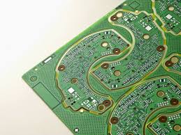
What size restrictions exist for PCB prototypes?
In addition to the physical size of the pcb prototype, there are also other design constraints related to the components that must fit within the available space. High-density designs that feature surface-mount components or require tight component placement may need to take into account the size of the board as well as the spacing between components. Very small PCBs, such as those used in wearable electronics or miniature devices, might require special handling during both the fabrication and assembly stages. These boards may have size constraints based on component placement, which can impact the overall design and functionality. For example, smaller PCBs may require more precise fabrication processes to ensure that components are placed correctly and that electrical connections are intact.
When dealing with PCB prototypes that are larger than standard sizes, there may also be limitations related to shipping and handling. Larger PCBs are more prone to damage during transportation, and they may require special packaging to protect them during shipping. Additionally, the larger the PCB, the more expensive the manufacturing and shipping costs are likely to be, especially if the prototype requires specialized materials, surface finishes, or additional testing. For this reason, many manufacturers offer price breaks for smaller prototypes, but larger designs can become exponentially more expensive.
Moreover, manufacturing techniques such as panelization can also affect the size restrictions for PCB prototypes. Panelization is the process of grouping multiple smaller PCBs together on a larger sheet (panel) to increase efficiency during production. While this can help reduce costs for mass production, it may not be suitable for all prototype projects, especially if you are testing a unique design that doesn’t fit well with standard panel sizes. In such cases, individual PCBs may need to be fabricated and tested separately.


